


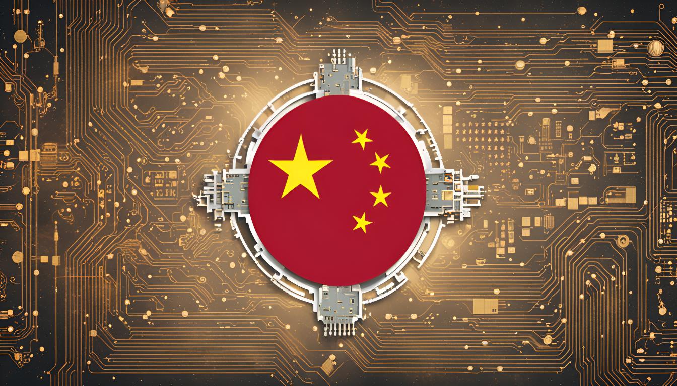
- China has secretly built a working prototype of an advanced EUV lithography machine, a critical tool for manufacturing cutting-edge semiconductors.
- The project, described as China's "Manhattan Project," involved reverse-engineering by former ASML engineers working under aliases in a secure Shenzhen facility.
- The prototype can generate EUV light but has not yet produced functional chips, with a realistic target for chip production estimated for 2030.
- The effort is a central part of China's six-year push for semiconductor self-sufficiency, coordinated by Huawei and aimed at removing U.S. influence from its supply chains.
- The development challenges long-standing U.S.-led export controls designed to prevent China from acquiring such advanced chipmaking technology.
In a high-security laboratory in Shenzhen, Chinese scientists have achieved a technological milestone that Western powers have spent years and billions of dollars trying to prevent.
According to exclusive reports, China has secretly built a working prototype of an extreme ultraviolet (EUV) lithography machine—the indispensable, astronomically complex tool required to manufacture the world’s most advanced semiconductors. Completed in early 2025 and now undergoing testing, this prototype represents the culmination of a clandestine, state-directed effort described by insiders as China’s modern “Manhattan Project.” The development signals a potential shift in the global balance of technological power, challenging a core Western strategy of containing China’s rise through export controls on critical machinery.
The crown jewel of chipmaking
EUV lithography sits at the apex of modern industrial technology. These machines, which can cost over $250 million each, use beams of extreme ultraviolet light to etch circuits onto silicon wafers at a scale thousands of times thinner than a human hair. This capability is fundamental for producing the powerful chips that drive artificial intelligence, advanced weapons systems and next-generation consumer electronics. For decades, this technology has been the exclusive domain of a single company: ASML Holding NV of the Netherlands. A concerted U.S. foreign policy effort has successfully blocked ASML from ever selling an EUV system to China, creating a chokepoint in Beijing’s ambitions for technological self-reliance.
Inside China’s “Manhattan Project”
The reported breakthrough is not an accident of open research but the result of a highly classified, state-mandated program. Sources indicate the project leverages extensive reverse-engineering of ASML’s technology, spearheaded by recruited former ASML engineers—many of them Chinese-born veterans of the Dutch firm. To maintain secrecy, these engineers reportedly work under aliases within the secure Shenzhen compound, with teams isolated from one another. The recruitment drive offered substantial financial incentives, part of an aggressive national strategy launched in 2019 to attract global semiconductor talent.
The electronics giant Huawei plays a central coordinating role, managing a sprawling network of companies and state research institutes. The operational culture mirrors a national security lockdown: employees on sensitive teams often sleep on-site, have restricted communication and work under constant surveillance. This intense, compartmentalized environment underscores the project’s strategic priority for the Chinese Communist Party, which views semiconductor independence as a cornerstone of national security and economic sovereignty.
A long road from prototype to production
While the existence of a light-generating prototype is a significant symbolic and technical achievement, analysts caution that major hurdles remain. The machine is described as much larger and cruder than ASML’s refined systems. The most daunting challenge lies in replicating the precision optics—specialized mirrors produced by firms like Germany’s Zeiss—that are essential for reliable, high-volume chip production.
- China is reportedly sourcing critical components through secondary markets, salvaging parts from older ASML machines, and using intermediary companies to obscure procurement.
- The official target is to produce working chips by 2028, but sources close to the project suggest 2030 is a more realistic timeline.
This progress, however slow, contradicts recent assurances from ASML’s leadership. In April 2025, CEO Christophe Fouquet stated China would need “many, many years” to develop comparable EUV capability. The prototype suggests Beijing’s timeline may be accelerating, fueled by a vast allocation of resources and a willingness to circumvent Western export controls through espionage, recruitment and gray-market networks.
A new phase in the Tech Cold War
The development carries profound implications for global security and industry. Historically, control over foundational technologies like EUV lithography has allowed the United States and its allies to maintain a generational lead in computing and military hardware. China’s relentless push toward indigenous capability threatens to erode that advantage, potentially enabling Beijing to produce advanced chips for AI and surveillance systems free from foreign restraint. The project’s stated ultimate aim, according to a source, is for China to make advanced chips on entirely China-made machines and to have “the United States 100% kicked out of its supply chains.”
An unfolding strategic challenge
The revelation of China’s secret EUV prototype marks a pivotal moment in the ongoing technological standoff between Washington and Beijing. It demonstrates the limitations of an export-control regime in the face of a determined, well-resourced adversary employing a whole-of-nation approach. While significant technical and manufacturing obstacles remain, the prototype proves that China’s path to semiconductor self-sufficiency, though long and arduous, is being paved. The world now watches to see if this secret project in Shenzhen can transition from a laboratory proof-of-concept to the foundation of a truly independent—and competitive—global chipmaking industry.
Sources for this article include:


Please contact us for more information.


